
Syncopated Systems™
Seriously Sound Science™
|
Syncopated Systems™
Seriously Sound Science™
|
| Home | Services | Case Studies | About | Library | Contact |
Common Threads: Media, Science, Technology, and Other MagicMay 2020: The COVID-19 Chronicles Early Computers
Drs. J. Robert Oppenheimer and John von Neumann in October 1952 with the IAS Machine at the Institute for Advanced Study (IAS) in Princeton, NJ The history of electronic computers began nearly seven months before Japan’s attack on Pearl Harbor prompted the United States to enter World War II. Interestingly, and perhaps with some irony, electronic computers were used to create the atomic bombs that were dropped on Japan, bringing the end of World War II nearly four months after the fighting ended in Europe. In little more than 25 years, computers migrated from machine rooms to the Moon and back. Major milestones include the following:
The Apollo Guidance Computer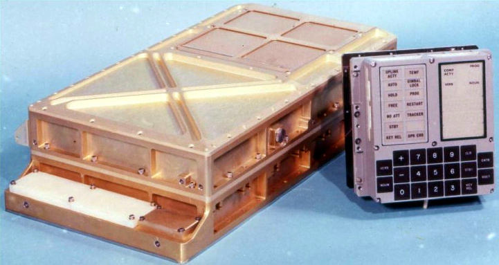
Apollo Guidance Computer with DSKY (display and keyboard) user interface unit Last year (2019) marked the 50th anniversary of the first people landing on the Moon. Among the celebrations, some of my friends—including volunteers for the Computer History Museum—undertook a project to restore and demonstrate the operation of an Apollo Guidance Computer (AGC). Flights to the Moon starting with Apollo 9 in March 1969 included two Apollo Guidance Computers: one in the command module (CM) and one in the lunar module (LM). (In December 1968, Apollo 8 orbited the Moon but did not carry a lunar module.) The user interface was via a DSKY (“display and keyboard”) data terminal; each lunar module had one DSKY and each command module had two DSKY data terminals, on the main instrument panel and in the lower equipment bay near a sextant used for aligning the inertial guidance platform. My friends had arranged to borrow an AGC from a former Apollo program worker in the Houston area who had later purchased about 2.5 tons of surplus material from the program. They had a narrow window of opportunity and an even shorter deadline. 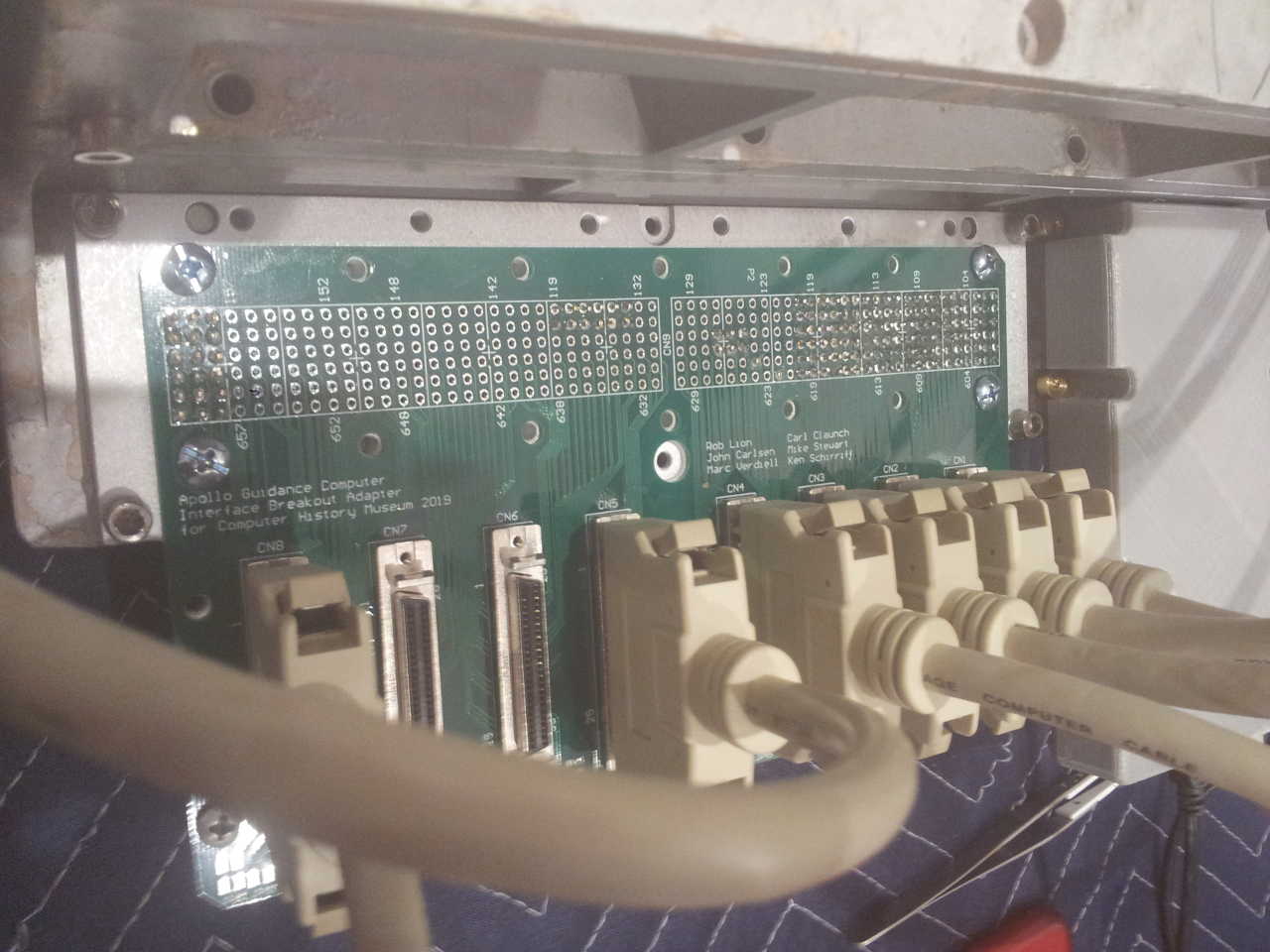
The printed circuit board I designed, connected to the front of the Apollo Guidance Computer in 2019 To run their simulations and demonstrations, they needed to make electrical connections to the AGC via its spacecraft connector (pictured, in white). By doing this, they would be able to simulate inputs expected by an AGC while connected with the rest of a spacecraft. They needed a printed circuit board (PCB) designed quickly. As a long-time committed computing technology consultant, researcher, and developer, I have the tools, training, and experience to do design circuits and PCBs reliably and efficiently, so I volunteered to help. (The machined aluminum frame was created by the accomplished mechanical designer Rob Lion.) My First Look at an AGCThe first time I had seen an AGC was about 10 years earlier, when I lived Texas and had attended a function at the Lyndon Baines Johnson Library and Museum (on the campus of the University of Texas at Austin). This must have been in 2009, which was the 40th anniversary of the first Moon landing and a year after both the 50th anniversary of the creation of NASA and what would have been LBJ’s 100th birthday. At the time, the museum included a temporary exhibition titled To the Moon: The American Space Program in the 1960s, and one of the displays included an AGC. 
Apollo Guidance Computer user interface The AGC Data TerminalOne of the first things to impress me about the AGC was its user interface: the “display and keyboard” (DSKY) unit. This includes push buttons marked “noun” and “verb”, which revealed to me that the system was object-oriented in its design. The ideas behind this term represent major advances in computer science, still new at the time, having first emerged at MIT in the late 1950s and early 1960s. Original DSKY units each included a green high-voltage electroluminescent display with seven-segment numerical digits. Electroluminescent displays are rugged but they don’t have long lifespans. So, for the 2019 demonstration project, a working replica of the DSKY user interface was created (by our good friend Ed Thelen) using green seven-segment light-emitting diode (LED) modules. (Visible LEDs weren’t invented until 1962, and they were only available in red until after the invention of green LEDs in 1972. I can vaguely recall how the variety of available LED colors, shapes, and sizes expanded after I started buying electronic components as a kid in 1979.) AGC Chip-Level IntegrationThe AGC introduced a major step in the integration of automatic digital electronic computers, a history that spanned only about 22 years. 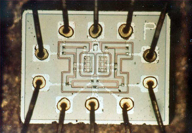
Fairchild dual 3-input NOR gate IC Each integrated circuit was of the same type, a device containing dual (two) three-input NOR gates. The NOR gate and its mathematical dual the NAND gate (a contraction of NOT and AND) are each functionally complete operators in that all logical operations (AND, OR, and NOT) may be constructed with each type of those logical gates. In the “Block I” version of the AGC were 4,100 integrated circuits. The “Block II” (1966) version had only 2,800 integrated circuits. (Having six transistors in each integrated circuit, the total number of transistors in the integrated circuits of these versions would have been 24,600 and 16,800, respectively.) These integrated circuits were manufactured by Fairchild Semiconductor, where the modern silicon monolithic integrated circuit was invented in 1959 by co-founder Dr. Robert Noyce (1927-1990). (The prior year, a germanium hybrid integrated circuit had been invented at Texas Instruments by Jack Kilby, 1923-2005.) While growing up in Silicon Valley, I knew of two former Fairchild fabrication facilities, either of which could likely have been where these components were likely made—one in Mountain View and one on Bernal Road in south San Jose. I knew these as closed, fenced off, and allegedly toxic waste sites. (I recall learning that Silicon Valley had 26 toxic waste Superfund cleanup sites, and that 24 of these were directly related to the semiconductor industry.) 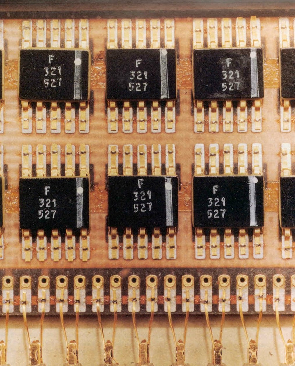
Fairchild dual 3-input NOR gate ICs in flat packs on AGC PCB AGC Board-Level IntegrationEven the printed circuit boards (PCBs) in the AGC were advanced for their time, and the integrated circuits were packaged so that they could be surface-mounted, a method that would not become common for about 25 years. The process of printing circuit boards had been invented for the United States Army in 1950 and (according to the patent) it was not commercialized until 1956. Until about 1970, printed circuit boards usually had only one conductive layer, apparently due to the extra difficulty and cost of aligning conductive layers on both sides and and making reliable vertical interconnections (usually with small metal-plated but otherwise empty holes called vias). As I recall, printed circuit boards carrying integrated circuits in surface-mounted packages were not common until the late 1980s, and printed circuit board assemblies with roughly equal mixes of surface-mounted and through-hole devices were common into the early 1990s. Read-Only MemoriesRead-only memory (ROM) is an important type of memory because it is stable. This is particularly important in space, where there is no planetary atmosphere to slow cosmic rays that can cause a soft error such as a flipped bit in semiconductor-based random-access memory (RAM). Semiconductor ROM integrated circuits offered a cost-effective means of distributing computer programs for decades. As a result, these devices were the dominant media used to distribute software for video games from the introduction of replaceable ROM video game cartridges in 1976 until CD-ROM became a cost-effective alternative in the mid to late 1990s. Manufacturers of ROMs printed each customer’s finished patterns into their devices’ top layer of metal (a method called mask programming), and realize economies of scale by selling the rest of the design to multiple customers. Developing Patterns for Read-Only Memories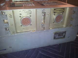
Rear of the Apollo Guidance Computer with core rope (ROM) emulation modules Developing the patterns to be printed into ROMs generally require special hardware that would emulate how the ROM would work while still allowing the software developer to change its contents quickly. Having the emulation units may not have been necessary for the demonstration, but having them allowed different versions of the software to be run. Emulating ROM is something that I became very familiar with. Early in my career, I worked for video game pioneers Atari and Activision, and the industry’s creator, Atari founder Nolan Bushnell (born 1943). I later co-founded video game developer Iguana Entertainment, where my work (1991-1996) primarily involved creating similar hardware for ROM emulation and cross-platform interfaces to enable software development, in much the same way that Activision and Raytheon had built their own ROM emulation systems (circa 1979 and 1963, respectively). My hardware connected (at first) Commodore Amiga and (later) IBM PC-compatible computers to the video game consoles that were new at the time, primarily the Super Nintendo Entertainment System (SNES), Sony PlayStation (PSX/PS1), Sega Saturn, and (to a lesser extent) Atari Jaguar and Sega Genesis. 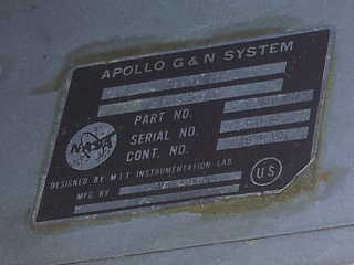
Rear plate on the AGC borrowed in 2019 reading “APOLLO G & N SYSTEM” (guidance and navigation system) and “DESIGNED BY MIT INSTRUMENTATION LAB” In late 1990, such development hardware could be purchased from Nintendo at a cost of $60,000 per station. Nintendo later offered a cost-reduced unit for only $15,000. These prices were out of reach for small developers, so I created interfaces that performed better and—by leveraging and reworking production consoles—could be produced for under $500. (I also made a simpler interface that allowed graphical and audio artists to proof their work, which cost only about $50.) (After the release of the original Sony PlayStation in late 1994, I had reverse-engineered it so thoroughly to make my interfaces that Sony later hired me to design a low-cost PlayStation to establish an official brand presence in emerging markets. Designing and budgeting for 25-million units had their own interesting joys and challenges, as did working for the world’s fifth-largest media conglomerate.) With the last version on my SNES interface, I was able newly-available technologies allowed me to put the ROM emulation memory into a cartridge that could be used independently for play testing or demonstrations. Although I already had my eye on flash EEPROM, it was still relatively new, complex to integrate, and expensive compared with a new type of “pseudo static” random-access memory (PSRAM) from Toshiba, which was essentially DRAM and refresh counter on the same integrated circuit. To use the Toshiba PSRAM, I needed to create very small switching power regulators, which I was able to do with a new line of integrated circuits from Maxim Integrated Products, which I had become familiar with when I started using its single-supply RS-232 level translators in 1989 and because it was based near my childhood home in Sunnyvale. (At the time, getting the right inductors was tricky.) The Toshiba PSRAM integrated circuits also required a refresh controller that I implemented in programmable logic devices (PLDs) from Lattice Semiconductor; at first I planned to use a new “zero power” variety, which I ultimately didn’t need because I found a way to turn off the power to the PLDs when the cartridge was not active. 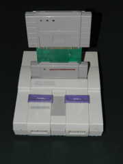
My cross-platform software development interface for the Super Nintendo Entertainment System (shown with 32 Mib/4 MiB ROM emulation cartridge) I designed the original cartridge to store only up to 16 Mib (2 MiB) plus a small area of user data (configured with DIP switches on the back of the cartridge) after my boss (the president of the company) assured me that our company would never make a larger game and directed me to use the through-hole version of the Toshiba PSRAM, despite my assurance that the same integrated circuit was inside both packages. It wasn’t long before the memory footprint of one project exceeded its original budget and I needed to design a modification and rework cartridges to allow them to store up to 24 Mib (3 MiB). The rework involved stacking a second PSRAM (in a 0.600-inch-wide DIP package) in two locations (and connecting the chip select terminal separately)—just as I had done as a kid modifying Atari hardware—and (to provide the additional chip select signals) stacking an extra Lattice GAL16V8 PLD in a PLCC. I then cut away just enough of the plastic on the back of the cartridge shell to accommodate the stacked components, and covered them with large paper labels to create a new protective surface. All things considered, the redesign and rework were quick, inexpensive, and not terribly ugly. (At that job, I had also quickly made some one-off circuits that were highly functional and very inexpensive—though certainly less elegant—including a breakpoint trigger for the Motorola 68000 in the Sega Genesis, an advanced automatic breakpoint trigger for the SNES, and an RGB-to-NTSC video encoder for the Sega Titan arcade system board.) Ultimately, I was able to create a new cartridge with a capacity of the console’s maximum addressable space of 32 Mib (4 MiB) by using all surface-mounted integrated circuits. I also improved the efficiency of the power regulation circuit by replacing the inductor with one having toroidal shape and more-ideal size. I purchased these directly from their manufacturer Gowanda Electronics; their smaller size, higher performance, and low per-unit cost allowed me to justify a minimum order quantity that was significantly more than I would ever use. This is also one example of how large a part supply chain management plays in board-level circuit/product development, how I entered operations management, and how I had already combined development and operations roles 15-20 years before the emergence of the term DevOps. Historical Capacities of Interactive Electronic Distribution Media
Computer/Video Game Distribution Media Capacities by Year On September 23, 2019, I gave a presentation about trends in storage in video games and computer games—collectively also known as interactive electronic entertainment software—at the Storage Developer Conference (SDC), which is hosted by the Storage Networking Industry Association (SNIA). My 2019 presentation at SDC (available here in PDF) built upon a presentation I gave earlier at the Flash Memory Summit (FMS) in August 2017, which was also in Santa Clara. I first charted the sizes of distribution media capacities in 2006—30 years since video game software was first distributed on cartridges—while developing an application programmer interface (API) for Sony that optimized data access from the Blu-ray disc (BD) drive on its PlayStation 3. (By the time I joined the project, the API was nearly complete but each new revision needed to be thoroughly tested on the three platforms it supported. I also wrote software that demonstrated its efficacy.) That technology, now 14 years old (and spanning nearly one-third of the history of the video game software market), brought with it the last significant increase in the capacity of distribution media for video games. With the spread of internet-based software distribution came considerable decreases in value to consumers. Perhaps the most noticeable is that the software, which is larger and more complex than ever, is being tested and debugged less thoroughly. In at least some cases, game programs will not start until they have access to the internet and can verify that the latest patches have been downloaded and installed; this causes additional delays when network servers are overloaded during peak market demand, such as after new games are received as Christmas gifts. 
Computer/Video Game Industry Revenue by Year Although the annual revenues of the video game industry (see chart) now rival those of the motion picture industry, this lack of quality (even if only temporary) is particularly perilous because it repeats the underlying cause of the video game crash of 1983. Next article in this series: The First Microprocessors Previous article in this series: The Space Race Back to series index: Common Threads index |
| Syncopated attempts to present a model Web site that meets or exceeds all applicable technical and legal requirements, including those of the A.D.A., COPPA, GDPR, ICANN, and W3C. | Syntax validated |
Style sheet validated |
Highest accessibility |
| “Syncopated Systems” and “Syncopated Software” are registered trademarks, the interlaced tuning forks device and the “seriously sound science” and “recreate reality” slogans are trademarks, and all contents (except as otherwise noted) are copyright ©2004-2026 Syncopated Systems. ALL RIGHTS RESERVED. Any reproduction without written permission or other infringement is prohibited by United States and international laws. | |||